
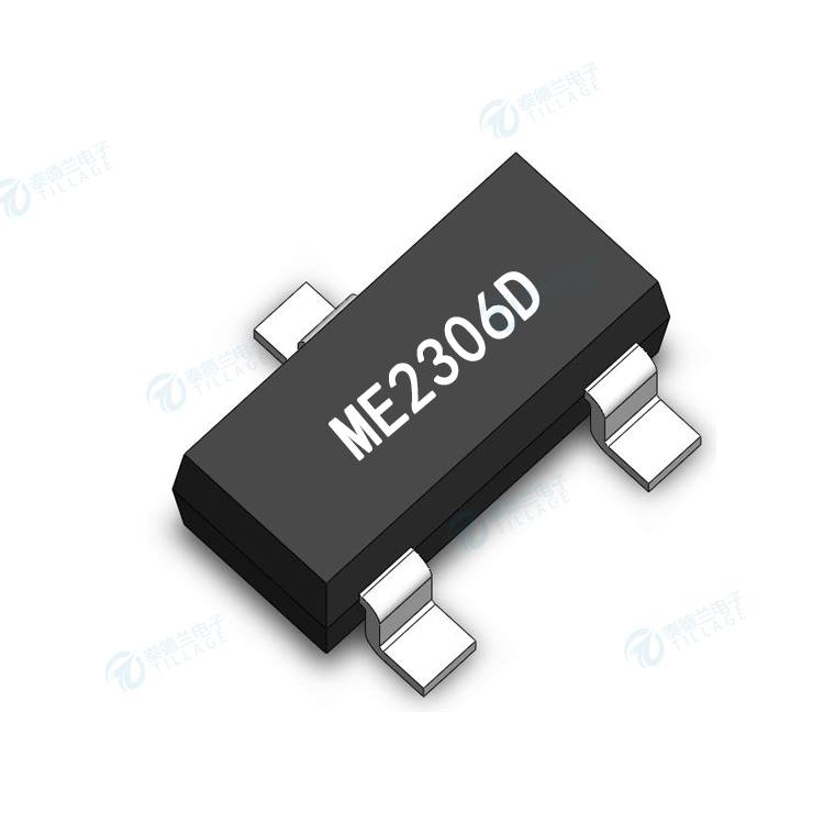
ME2306D一般说明
ME2306D 是 N 沟道逻辑增强型功率场效应晶体管,采用高单元密度、DMOS 沟槽技术生产。 这种高密度工艺特别适用于最大限度地减少导通电阻。 这些器件特别适用于低电压应用,例如蜂窝电话和笔记本电脑电源管理以及其他需要高侧开关和低在线功率损耗的电池供电电路,这些电路采用非常小的外形表面贴装封装。
ME2306D应用
● 笔记本电源管理
● 便携设备
● 负载开关

GENERAL DESCRIPTION
The ME2306D is the N-Channel logic enhancement mode power field effect transistors are produced using high cell density , DMOS trench technology. This high density process is especially tailored to minimize on-state resistance. These devices are particularly suited for low voltage application such as cellular phone and notebook computer power management and other battery powered circuits where high-side switching , and low in-line power loss are needed in a very small outline surface mount package.
APPLICATIONS
● Power Management in Note book
● Portable Equipment
● Load Switch
特征
● RDS(ON)≦31mΩ@VGS=10V
● RDS(ON)≦52mΩ@VGS=4.5V
● ESD 保护
● 超高密度电池设计,RDS(ON) 极低
● 出色的导通电阻和最大直流电流能力
FEATURES
● RDS(ON)≦31mΩ@VGS=10V
● RDS(ON)≦52mΩ@VGS=4.5V
● ESD Protected
● Super high density cell design for extremely low RDS(ON)
● Exceptional on-resistance and maximum DC current capability
留言0